

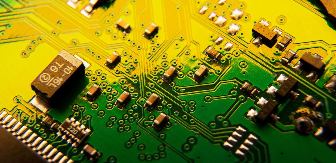
What is PCB Design?
PCB stands for Printed Circuit Board.
A PCB Design is the process of creating the layout and electrical connections of a circuit on a flat board using conductive pathways, pads, and tracks made of copper.
These boards hold and connect electronic components such as resistors, capacitors, ICs (Integrated Circuits), sensors, and microcontrollers in a compact and organized way.
In simple words, PCB design is like creating a roadmap for electricity — it decides how current will flow between components in an electronic device.
Types of PCB
1.Single-Sided PCB
This type has only one layer of copper on one side of the board. It is used for simple circuits like LED lamps or small power supplies.
2.Double-Sided PCB
Copper layers exist on both sides of the board. It allows more complex circuit designs, like in amplifiers or small robot controllers.
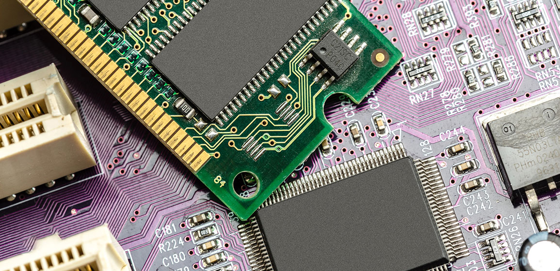
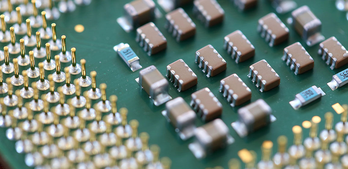
3. Multi-Layer PCB
Contains three or more copper layers stacked together with insulation in between. Used in high-speed and advanced electronics like computers, smartphones, and robotic systems.engineers to design complex shapes like airplane wings and car bodies with exact measurements.
4.Rigid PCB
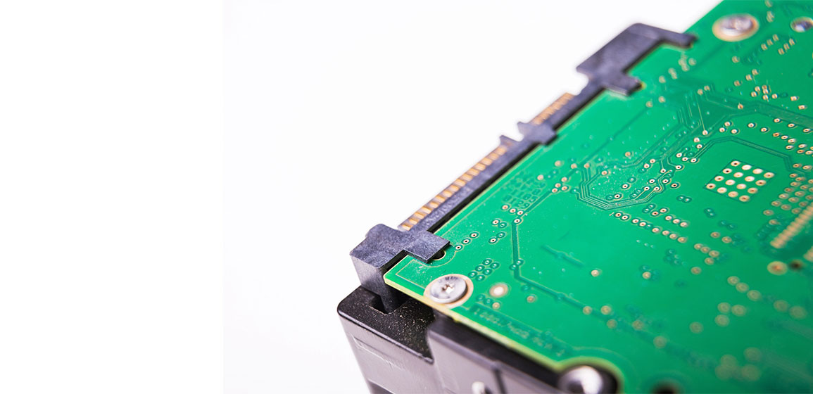
Made from a solid substrate (like fiberglass), it cannot bend. Common in desktop computers, TVs, and heavy machinery.
5. Flexible PCB
Made from flexible materials, these boards can bend or fold, used in wearable devices, cameras, and robotics where space is tight.
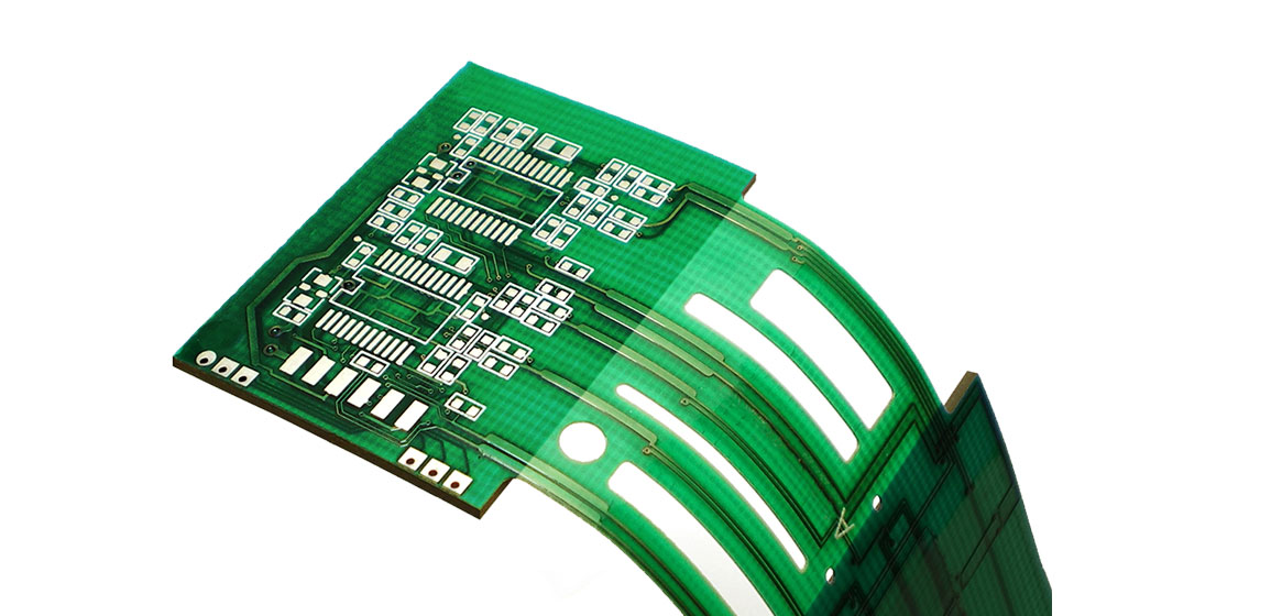
6. Rigid-Flex PCB
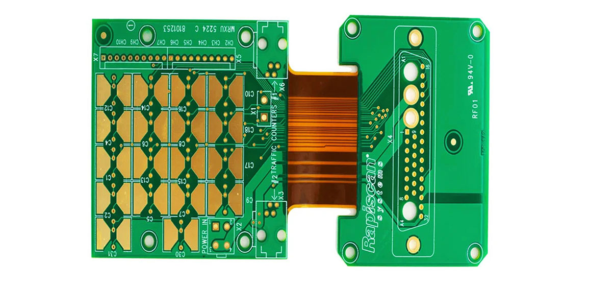
Combination of rigid and flexible PCBs. Used in advanced military, aerospace, and robotic systems where flexibility and durability are needed.
Why PCB is Important?
Foundation of Every Electronic Device:
Every electronic device from your smartphone and smartwatch to industrial robots and satellites depends on PCBs to function. They act as the structural base that holds all components in one place, ensuring stability, organization, and continuous electrical connectivity. Without a PCB, connecting and maintaining complex circuits would be nearly impossible.
Ensures Electrical Accuracy:
PCBs are designed with precision-engineered copper pathways that control how current flows between components. This ensures consistent voltage levels, reduces signal loss, and prevents short circuits. As a result, PCBs help maintain the accuracy, timing, and performance of sensitive electronics like sensors, processors, and controllers.
Supports Miniaturization:
In today’s world, devices are getting smaller but more powerful and that’s possible only because of PCB technology. Multi-layer PCBs allow engineers to stack multiple circuits within tiny spaces, optimizing performance without increasing size. This is what makes modern gadgets like smartphones, wearables, and compact robots possible.
Improves Performance and Reliability:
Well-designed PCBs use optimized layouts that minimize electrical noise, heat generation, and interference. This not only ensures smoother signal transmission but also improves the overall reliability and lifespan of the device. Components remain securely fixed, reducing the risk of loose connections or breakdowns over time.
Simplifies Assembly and Maintenance:
PCBs make circuit building systematic every component has a defined place, label, and connection path. This simplifies the assembly process and makes troubleshooting much easier. Engineers can quickly identify faulty parts, replace them, and restore the circuit’s functionality with minimal effort and time.
Enables Automation and Innovation:
From industrial automation to smart robotics and IoT devices, PCBs enable intelligent control and data communication between sensors, processors, and actuators. They form the backbone of innovation by integrating hardware and software efficiently, helping machines think, act, and respond automatically.


